Troubleshooting Conway's Game of Life to Completion

It's been a long time since my last post. School is always rough, never enough free time, and even when you do have said free time, you don't always want to spend it being productive. But that outta the way, here's the conclusion to my Conway's Game of Life series of posts.


It's time to talk about troubleshooting! This is a continuation of my Conway's Game of Life series, continued from the Architectural promised land.

The Need to Troubleshoot

One of the most important parts of design and implementation. Things, especially complex things, rarely go according to plan on our first attempts and we have to be capable of figuring out what went wrong and how to fix it.

Another thing I know many people face is the willingness to go to the debugger in programming, or in this case the simulator. I've observed in myself and my class mates a very strong aversion to using the simulator to figure out what is wrong with our SystemVerilog or Verilog designs. Rather, we prefer to waste hours on end trying to fix the problem by just looking at the code and figuring out what is wrong.

This will invariably take longer than it needs to, and you will almost inevitably end up using the simulator and figuring out the problem in much less time anyways, so you may as well use it right off the bat.

Troubleshooting Conway

Because the whole design just runs without any user interaction, simulating it requires only the simplest testbench, with just a clock being input into the test module. The first, and main, roadblock I ran into was the size of my block rams.

What I wanted to do was follow each pixels data through the whole path and look at the values being read and written and from which locations in memory they were being read from and written to. This would allow me to find all of the potential off by one errors in the design.

The block rams were too large though, and the simulator built into the Vivado Design Suite would not open the block ram for me to look at it. This would actually turn out to be a huge blessing in disguise though since it would greatly simplify the troubleshooting process.

Scaling the Problem

What could I do without having to change large portions of the design I already had? I could make the block ram only be a 4x4 square of cells instead of a 640x480 grid of squares. I wouldn't have to change the VGA driver to get this to work at all, since I could just send the 2 MSBs of each address request to the video ram. So I ran with that idea, scaled down the size of the block ram and started trouble shooting the transfer logic.

Transfer Logic

I don't remember what the actual specific problem was for the transfer logic, but it was definitely an off by one error. Sometimes with designs like these, specially when you're new to this sort of stuff, it can be hard to remember what values are being presented where, and on which clock cycles. This is a problem depending on where you are incrementing values. Using the small 4x4 grid allowed be to easily see where the problem was and correct it, making the transfer logic work perfectly in a short period of time.

The actual game logic was not nearly so simple...

Fixing the Game Logic

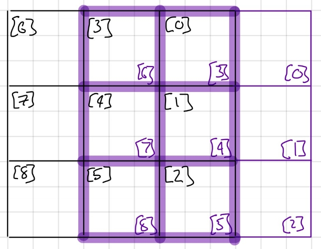
Looking at fixing the game logic, even with the board shrunk down to 4x4, was daunting. So the first thing I did was draw out the entire board, with its initial state. I then calculated by hand the next state of each cell, along with the coordinates and memory address of each cell for easy reference when I was looking at the outcome in the simulator.

Conway Board - By Hand.jpg

In the center of each cell is the initial state, with the surrounding cells values being written around it to ease calculation of the next state, in the bottom left is the ram location, and the top right is the next state of that cell. This diagram was invaluable in checking the effectiveness of my design.

Going through every clock cycle to check every read and write being done by the game logic module was extremely tedious, but in the end it was the easiest and fastest way to find the errors in my logic. It was like the transfer logic, in that I was not taking into account different values to presented along with counters being incremented too soon. You can see the value at the top of each cell, is the time in the simulator where the calculation of that cell started, to ease finding it again after changes were made.

When all of the logic, for every location on the 4x4 grid, was checked and known to be working, I implemented the design to run on the Basys 3 and see what it looked like on the tv.

It's like some sort of seizure machine, which scared me at first, but I realized that the speed at which the board was changing and the size of the pixels were causing this, and that most likely it would look fine at the real resolution I wished to run the game at.

Completion of the Project

I know this post was a long time coming. I will strive in the future to write more consistently, which will allow me to go into more detail as well (who knows if anyone wants this).

In the end, this was an incredibly exciting project. I pushed myself to come up with clever ways to solve limitations I placed on myself which gave me quite a few learning opportunities. Writing all of these blog posts was also a learning opportunity. I know my writing isn't the best, but writing more will lead to improvement.

And here is the final product.

All of the files for this project are located here, and let me know if you have any suggestions for improvement, of which there are probably many, or if you have any questions about its operation.

Architecture for Conway's Game of Life on an FPGA

It's finally time to talk architecture! This is a continuation of my Conway's Game of Life Adventure, continued from the VGA chat.

Requirements

Before we can start we need to talk about requirements. Let us first define the rules of the Game of Life, copied from Wikipedia.

  • Any live cell with fewer than two live neighbours dies, as if caused by underpopulation.
  • Any live cell with two or three live neighbours lives on to the next generation.
  • Any live cell with more than three live neighbours dies, as if by overpopulation.
  • Any dead cell with exactly three live neighbours becomes a live cell, as if by reproduction.

Right up front we know we need to know the status of 9 cells, the cell we are interested in, plus the 8 around it, to find the next state of that cell.

In the lab document that Conway's Game of Life was chosen from, the problem was described as having to be run on an 8x8 LED Matrix. But if you've read my project decision posts, you know I have rather lofty goals. I want to run this game at full standard VGA resolution of 640x480. I also very much would like to run the game at 60 in-game "ticks" per second to match the screen refresh of 60Hz.

The primary limitation I am placing on myself is that I want all of this to happen on my Basys 3 board, using a Xilinx Artix-7-A35, which only has 1800kb of block ram. The assignment presumes you will be using the Terasic DE1-SoC that we were assigned at the beginning of the term, which is has roughly 4 times as much available logic.

Dead Ends

Looking back at our previous two projects, we had to make a stripped down version of tug of war, where we used the strip of LEDs on our dev boards, and you would have two people press buttons and the LED that was lit up would move around. We were told to implement this using a module for every light, and have all the modules be wired together. This method just won't work for the Game of Life based on the requirements I have laid out above. Even if each module only used part of one logic slice, I've only got 5k logic slices and 302k cells I want to model.

The First Step

Rather than use a separate module for each "cell" in my game, which is the massively parallel option, I realized the only way for me to get this working on my Basys 3 was to use block rams to store the current and next state. A 1 bit wide and 307k address long block ram, built out of cascaded 32k block rams was the answer. Though I didn't end up only using 307k addresses, making the addressing scheme easier by using X and Y coordinates concatenated together lead to needing 19 bits of addressing and 524k addresses. This means each ram we use will require 16 of the 50 available block rams on the board.

Two Naive Approaches

The first approach I attempted was extremely naive. I figured if I need to read 9 cells to calculate the next state for 1, I would just infer 9 read ports on my ram. I justified this in the short term in my head by the fact that we would be using so many cascaded block rams and each one has 2 read ports, I figured it might work. Well when I tried to implement the design it attempted to use distributed memory and very quickly ran out of available logic slices, which meant my attempted 9 read port cascaded block ram wasn't a viable option. You live and you learn I guess.

We know we need to read 9 cells status in order to determine the next state of any given cell. So my next idea was to run the clock for the overall design at 9 times the speed of the pixel clock for the VGA, or 225MHz. This would allow us to read 9 addresses in the time it would take the output to draw one pixel, allowing us to keep pace with the drawing of pixels when we are calculating the next state of the pixels. It would later turn out that at least 10 clock cycles would be required, but it would end up not mattering anyways. The problems here arose when just testing out the VGA driver displaying a random set of data loaded into the block ram. When running the block ram at 225MHz, the design would fail timing. This is my first time running into a situation like this, but I think it has something to do with the fact that the block rams are spread out all over the FPGA, what with 16 of them being all cascaded together. The spread out nature of the cascaded block rams combined with the high operating frequency led to the timing failure.

Through continued experimentation I discovered that the highest integer multiple of 25MHz I could run the block ram at in this configuration was 150MHz. This means I needed to get more creative, the brute force approach of reading 9 cells for every cell just wasn't going to work, especially if I wanted to run the game at 60 in game "ticks" per second.

The Architectural Revelation

This wasn't a last minute revelation, I was just hoping to make the game logic simpler in exchange for making the it less efficient, but it would seem that wasn't meant to be. We know we need to read 9 cells in order to compute the next state of each cell, but as long as we compute the next states in a reasonable manner we can avoid having to read most of the cells for most of the next states being calculated. What I mean is that if we design our game logic to raster across the board in the same fashion as the VGA output will be doing, we can see that 6 of the cells for calculating the next state of the next cell are the same from the previous cell. This means we only need to read 9 cells, once, at the beginning of the row, and then for each consecutive cell in that row we can shift the previously read cells over and read in 3 new ones to do our next state calculation.

Conway Grid Example.jpg

Above, you can see an example of how the shifting of the cells will work. In black I have denoted the grid of 9 cells being read, with the status of the cells being loaded into a 9 bit long register. When you shift to calculate the next cell, denoted in purple, because of the way I have arranged which cells go to which bit in the register, we can just shift the bits 3 times to the left and then load in the 3 cells we need.

Data Flow

The first plan I had for the data flow model of the design was to use just two block rams, one for the present state and one for the next state. The game logic would use one as the present state, writing out to the other as the next state, and then would switch for the next frame, reading from what was previously the next state and writing to what used to be the present state. I would also have had the VGA Driver read from whichever was currently the present state. This plan had a lot of extra complexity, but would most efficiently utilize the resources on our board.

Knowing that our Artix-7-a35 has 50 available block rams and that each of the rams in our design will use 16 of them, we have space for 3 rams in the design. This is when I decided I would use a dedicated ram just for the video frame buffer, this way the VGA Driver will always be reading from the same ram. My original idea in this configuration was still to have the game logic switch back and forth, reading from one and writing to the other ram. It would also be writing to the frame buffer every time as well.

This is when I realized another potential problem with the design. If I were going to write to the VGA ram, the game logic would not be able to go faster than the display output, or it would end up over writing data for a given frame that had not been displayed yet. Sure I could have come up with some sort of control signal to tell the game logic when a row had finished being displayed so it could write over it, and then wait for the next control signal. A new idea came to mind though when I "saw" all of the extra rows at the bottom of the screen that are not being displayed. Could I copy all the contents from the next state ram into the present state and frame buffer rams after the next state was calculated but before the next frame needed to be drawn?

The Architectural Promised Land

Doing some back of the envelope math we can see that our goal of copying the contents of the next state ram into the present state and the VGA rams. At 150MHz, our clock period is 6.67ns. We will need 3x639 + 9 clock periods per row, times 480 rows, means the game logic will take roughly 6ms to complete. We will also need 307k clock cycles to transfer the data, which is roughly 2ms. Our budget for each frame is 1/60th of a second, or 16.67ms, which means we have plenty of time to get the logic and the transfer done before the next frame starts. This method decreases the efficiency of the design, but it also decreases the complexity of the reading/writing structure, as well as giving me the opportunity to write another module, to copy the data.

The game logic can start at the beginning of when the frame is being drawn, but we need to be careful about the copying logic. The copying logic wont actually fit into just the period during the extra rows at the bottom of the frame, it would take too long. We can however, start the copy process before the last row of the frame has been drawn, we just have to ensure we don't start too early, overwriting any rows that have not been displayed yet.

Conclusion

We started with a rather naive and brute force approach to this design, which luckily didn't end up working. This forced us to use our heads and come up with a better way to access the data we needed. I believe something close to the reverse happened when it comes to the data flow of the overall design though. We started with a rather complex reading and writing idea, only to realize we did not need all that extra complexity.

Unfortunately, architecting the design isn't the last step, it has to be implemented in SystemVerilog. My first attempt at this did not go well, which you can see in the youtube video below.

It would seem I made a great deal of what I would call off by one errors throughout my design. Whether they are in the game logic, or in the transfer logic, the cells are being shifted to the right and down. You can see some of the little flyers in there though, so it would seem that at its core the game logic is working.

Next time we can go into what I did to figure out what was wrong, and how I fixed it.

Making My Own VGA Driver In SystemVerilog

This is a continuation of my posts about my final project for EE271, continued from the Project selection process here, here, and here.

The first thing I wanted to get working in this design was the VGA output, as the whole design rests on being able to display the results on a monitor. Not to get too into the weeds of the overall architecture, but I knew I would be using cascaded block rams to create a 1 by 524k frame buffer for the output. 1 bit per pixel since it's only a black and white output, 10 bits for the x coordinate and 9 for the y coordinate, concat them together to create a 19 bit addressing system.

The first step was to figure out how the VGA signal is supposed to behave. I went to google and found an excellent, and very informative website called ePanorama that has a detailed page with timing information, as well as a calculator to figure out timings for different resolutions.

VGA was created a long time ago, during the time of CRT monitors, the time it took for the beam to travel back across the screen to display the next row had to be accounted for. As well as the time it takes for the beam to travel from the bottom of the screen back to the top to start the next frame. These times are referred to as the front porch, back porch, and sync time. What they lead to is an effective resolution that is larger than the 640x480 you will be displaying. The effective resolution then becomes 800x525. During the times outside of the display resolution you need to output a solid black signal, as many monitors and TVs use that time to calibrate the output to the signal being input. There is also a pulse presented on the horizontal and vertical sync lines during the blacked out periods to inform the monitor to go to the next line or back to the top of the screen. I also ended up finding another extremely useful document from a gentlemen named Eduardo Sanchez, called A VGA Display Controller, which i used for reference due to its many pictures and excellent explanations of the timing involved. This image in particular was very helpful to me.

Some things to keep in mind for this design are that because I am using the Basys 3 board, I have 3 4-bit dacs, one for each color, and also that the pixel clock for VGA output at 640x480@60Hz needs to be 25MHz. I was using a faster clock for the rest of the game, so I used a counter inside the VGA module to cut that down to the appropriate 25MHz. This will be covered in more detail in the next post about architecture.

The way I went about building up this design was to use a counter to keep track of x coordinates, that would increment with each pixel clock, and then increment the y coordinate counter each time the x coordinate reached its maximum. These coordinates would then be passed out as the address to the frame buffer block ram, which would return either a 0 or a 1, determining whether the output would be black or white for that pixel. There is also a check to determine whether we are inside the viewable region of the screen, and output black if we are not.

My first attempt at this design did not go particularly well, but it still sort of worked. I loaded the frame buffer with random 0s and 1s just to test the display output. I went and plugged it into a VGA monitor only to see the output shaking and shimmering around on the screen, it was there, but not a solid picture. As an aside, over the course of the term I had sort of gotten lazy about my next state logic and then turning the next state into the present state. I took a lot of shortcuts to save space in my code and this final project is where all that laziness came home to roost.

I don't have a video of shame to show you how this was borne out, nor do I have the original SystemVerilog to show you, but I will just say, it was bad. I decided then, to just start over with a blank slate. I went through and much more methodically determined next states, with separate transitions to those states. This diligence paid off, as the design worked the first time, displaying a solid image on the monitor when I plugged it in.

module v_driver(
    // Clock input
    input wire clk,
    // Data input to be displayed, 1-bit becuase its black and white
    input wire data,
    // Outputs to trigger the transfer of data and the calculation of the next frame
    output reg transfer_start,
    output reg logic_start,
    // Outputs for the VGA connector
    output wire [9:0] x_val,
    output wire [8:0] y_val, 
    output wire h_sync, v_sync,
    output wire [3:0] red, green, blue
    );
    // Parameters for the size of the screen
    parameter X_MAX         = 10'd639;
    parameter Y_MAX         = 9'd479;
    parameter X_SIZE        = 10'd799;
    parameter Y_SIZE        = 10'd525;
    parameter X_ZERO        = 10'b0000000000;
    parameter Y_ZERO        = 10'b0000000000;
    parameter COUNT_MULT    = 3'd6;
    
    // Registers to track the current and next position of the output
    reg [9:0] x_reg = X_ZERO, x_next = X_ZERO + 1'b1, y_reg = Y_ZERO, y_next = Y_ZERO;
    // Registers for the values of the color outputs
    reg [3:0] red_reg = 4'h0, red_next = 4'h0, green_reg = 4'h0, green_next = 4'h0, blue_reg = 4'h0, blue_next = 4'h0;
    // Registers to track the sync pusles both horizontally and vertically
    reg h_sync_reg = 1'b0, h_sync_next = 1'b0, v_sync_reg = 1'b0, v_sync_next = 1'b0;
    // Register to track whether the output should be enabled or not
    reg v_en;
    // Counter to divide the clock by 6
    reg [2:0] count = 3'b000, count_next = 3'b000;
    
    // Always block to clock through the next state of all the registers in the design
    always @ (posedge clk) begin
        count       <= count_next;
        x_reg       <= x_next;
        y_reg       <= y_next;
        v_sync_reg  <= v_sync_next;
        h_sync_reg  <= h_sync_next;
        red_reg     <= red_next;
        green_reg   <= green_next;
        blue_reg    <= blue_next;
        v_en        <= ( (x_reg < 10'd640) & (y_reg < 10'd480) );

        // Case block to output the read data from the memory or to output black
        // if we're outside the displayed portion of the screen
        case(v_en)
            1: begin
                    red_next    <= {4{data}};
                    green_next  <= {4{data}};
                    blue_next   <= {4{data}};
                end
            0: begin
                    red_next    <= 4'h0;
                    green_next  <= 4'h0;
                    blue_next   <= 4'h0;
                end
        endcase 
    end

    always_comb begin
        // Start the transfer at the 432nd line, so that the transfer wont over write anything
        // that hasn't been displayed yet but will finish as early as possible
        transfer_start = (x_next == X_ZERO & y_next == 10'd432) ? 1'b1 : 1'b0;
        // Logic will start calculating the next frame once the new frame starts
        logic_start = (x_next == X_ZERO + 1'b1 & y_next == Y_ZERO) ? 1'b1 : 1'b0;
        // sync pulses for ~90 pixels on the horizontal and ~2 pixels on the vertical
        h_sync_next = (x_reg > 10'd659) & (x_reg < 10'd756);
        v_sync_next = (y_reg > 10'd493) & (y_reg < 10'd496);
        // the counter to divide the clock by 6
        count_next = (count < COUNT_MULT - 1'b1) ? count + 1'b1 : 4'b0000;
        // Count x is the counter is at 5, increment y if x is at the end of the row
        // reset both to 0 if they reach the end of the screen
        y_next  = (x_reg == X_SIZE) ? ( (y_reg < Y_SIZE) ? y_reg + 1'b1 : Y_ZERO) : y_reg;
        x_next  = (x_reg == X_SIZE) ? X_ZERO : ( (count == COUNT_MULT - 1'b1) ? ( x_reg + 1'b1 ) : x_reg );
    end

    // Assign output registers
    // X and Y registers form the address for the memory to read
    assign red = red_reg;
    assign green = green_reg;
    assign blue = blue_reg;
    assign h_sync = h_sync_reg;
    assign v_sync = v_sync_reg;
    assign x_val = x_reg;
    assign y_val = y_reg[8:0];  
    
endmodule

Overall I think it was pretty valuable to write my own VGA driver. Sure I could have just used one of the professor's modules to do so, but I don't really like to abstract away things without at least learning how they work first. In this case, the easiest way to learn how it worked was to build it myself. It might not be the cleanest VGA implementation in SystemVerilog out there, but it is mine and it did the job I needed it to. I do wish I had used a version controlling system, so that the horror of my first attempt would be here for you all to see.

Tune in next time, when I will talk about the overall architectural design of the game, and several implementation problems I ran into.

The Project Selection Process Pt.3

Continued from Part 2.

I am sure at this point all of you are glued to your monitors in anticipation of what my project will be. At this point I was only 2 weeks out from the due date, so I decided to look over the options for lab ideas presented in the document for the final project. Most of the ideas were for simple games, all of which would be displayed on an 8x8 LED matrix. Things like frogger, flappy bird, guitar hero, etc. But amongst the crowd was a suggestion of Conway's Game of Life. In one of my programming classes we had made a version of the Game of Life and it was a good time. Also, if you had noticed, both of my previous ideas involved the real time analysis of information and loosely the Game of Life does as well, with the input being the previous output of the system.

Even though I was picking one of the projects listed in the lab document, I was already planning on expanding the scope of the project. Instead of running the game on an 8x8 LED matrix, I wanted to run the game at 640x480@60Hz out the VGA port. One of my TAs for the class told me that one of the other professors had a VGA module we could use to make it easier, but I knew I wanted to implement my own, even if just to use it as an additional learning opportunity. My interest in video also had me intrigued about implementing my own video output.

Now, with my project decided, we can move onto the fun part, how I actually implemented this beast.


The Project Selection Process Pt.2

Continued from Part 1.

We left off last time with me realizing I wouldn't be able to implement my video scalar. Someday though it will still happen, but it'll live in the projects list at 0% for quite a while I imagine.

My next idea came to me from another class I am taking this term, Systems and Signals in Continuous Time. I hadn't expected to enjoy this class, since I thought it was going to be another analog class in the same vein as circuits 1 and 2 at PCC, but it really surprised me. It is almost entirely about systems and signals in the abstract, I also had a fantastic professor, Professor Mari Ostendorf.

My idea was to create a real time FFT. I wanted to be able to plug in a music source, like my iPhone, and have it show frequency content, in bars, on a monitor. I knew going into this that there would be several road blocks to my success, but I was confident they would be surmountable.

The first was that I have not yet taken the discrete time version of the systems and signals class. This means I have not learned about the DFT or the FFT at all. I have only learned about the Fourier Transform in continuous time. The second is that I have not learned how to design digital circuits to manipulate floating point numbers, we only know how to do integer math, and even with that we've only explicitly learned how to do addition, though subtraction and multiplication are relatively simple offshoots of that.

This is when my work began in earnest. I only had 3 weeks or so till the final project was due at this point and I needed to start making progress. I began reading about the DFT/FFT and how they worked. I also started googling for means of performing the FFT using only integer math. This originally seemed very fruitful. I found several papers detailing means of doing the FFT using integer math and without the use of multipliers. As academic papers are though, they were incredibly dense and lacking in actual implementation details. They also had decidedly non-integer numbers in them. I would follow them up until they started talking about decimal numbers. I even went to Professor Ostendorf's office hours to see if she would be willing to help me out without using up too much of her time. She was very helpful, and went over several papers with me over the course of half an hour or so, but not enough progress was made, and I did not want to use up anymore of her time.

Long story short, the real time FFT idea had to go out the window as well. It will also be returning though! hopefully some progress will be made on this front during winter break!

check in next time to see what project was actually chosen.

The Project Selection Process Pt.1

Selecting a final project in a class can be tough. I know it very frequently is for me. It was particularly bad in my first digital design class here at the UW.

I attended Portland Community College for a little over a year before transferring, and in that time I had the opportunity to take 2 digital design classes. When I transferred though, they transferred for credit, but did not qualify for the first digital design class here, EE271. This is because at PCC they did not really teach us any Verilog, we did almost all our labs using 7400 series chips on breadboards. While here at the UW, they do almost all of the labs for this class in Verilog and implement them on FPGAs. They also do not have a separate Verilog course like I would have had I transferred to Portland State, so I was advised to retake the course in order to learn Verilog, since it would be expected that I would know it going forward.

What this lead to is me taking a course where I understood nearly all the concepts in advance. It allowed me to help my classmates a great deal, but it also gave me a long time to consider my final project.

A few weeks into the course I had an idea of what I wanted to do. I decided I wanted to make a video scalar. It would be able to accept composite video from something like an SNES and then output 1080p video over HDMI. Manipulating video has been something I have been very interested in since about 2011, when I started playing with video encoding on my own. So this project was something I was very interested in doing, and having personal motivation to work on it would be very valuable.

The problems began about a month before the end of the term when I started looking into how I would implement the design. The first stage of the design would be to digitize the signal. I haven't ever used them, but I know the Basys 3 has several XADC ports, and finding the Xilinx user guide on how to use them would be pretty easy. The difficult part would be interpreting, or demodulating, the composite video signal into something I could work with.

So I spent the better part of a weekend researching specifications of the composite video spec and found....almost nothing. There was so little information out there as far as signal specifications that I wasn't confident I would ever be able to move with the project. I decided maybe I could take in digital information over Display Port, at 240p, scale it up to 1080p, and output it over HDMI, but even that was turning out to be out of reach. I had really hoped to get some of my classmates to work with me on this project, and my attempts to recruit anyone were fruitless.

This project idea had seemed to meet a dead end, read on next time to hear about the next idea I considered.

My First Post and First Blog

My name is Chase and I'm currently a junior at the University of Washington in the Electrical Engineering program. I've wanted to start a blog off and on for several years and many different reasons but I finally got the gumption to do so now.

The purpose of this site will mainly be to document my own learning experience. Any time I work on projects relating to EE whether for school, or just for fun, I will probably write posts about it. Mostly as a learning opportunity and to learn from the wider community of the web if anyone decides to read what I have to say.

I don't pretend to be an expert, much of what I post will be amateur in nature and definitely have room for improvement, but that is what the site is for.

I am focusing on digital design here at school, so much of what I post will be about learning SystemVerilog, along with many projects related to FPGAs and rachitecture. I will also post about C or assembly programming periodically.

I currently own a Basys 3 FPGA dev board from Digilent, so for the time being most of my projects will be done in Vivado Design using SystemVerilog. I am looking at getting a Nexys Video as well, to give myself more room and better video output capabilities. I have no attachment to Digilent but this summer when I was looking for an FPGA board to play with and learn on, they had a great student discount and pretty good documentation, which couldn't be said about much of their competition.

Anyways, to anyone who made it this far, I commend you, and I hope that I post something you find interesting. Any and all feedback is welcome, I will be leaving comments on for now as well.


Chase